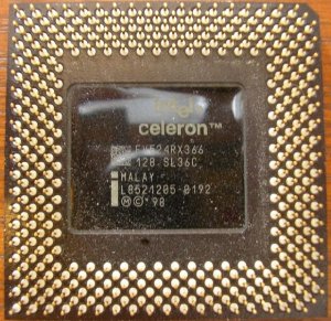
Starting with the 300A, all Celerons have come equipped with 128KB of on-die Level 2 cache running at full CPU speed and communicating externally via a 66MHz bus, making them far more capable than their sluggish predecessors.
Somewhat confusingly, all Celeron processors from the 300A up until the 466MHz were available in two versions – the SEPP form factor or in a plastic pin grid array (PPGA) form factor. The former was regarded as the mainstream version – compatible with Intel’s existing Slot 1 architecture – while the latter was a proprietary Pin 370 socket, neither Socket 7 nor Slot 1.

The use of a socket, rather than a slot, gave more flexibility to motherboard designers as a socket has a smaller footprint as well as better heat dissipation characteristics. Consequently, it provided OEMs with more potential to lower system design costs. The 500MHz version was available in PPGA packaging only.
The table below shows the various versions of the Pentium II Celeron processor between its launch in 1998 and its subsequent transition to use of a Pentium III core in 2000:
| Date | Codename | Transistors | Fabrication (µm) | Speed (MHz) |
|---|---|---|---|---|
| 1998 | Covington | 7,500,000 | 0.25 | 266/300 |
| 1998 | Mendocino | 19,000,000 | 0.25 | 300A/333 |
| 1999 | Mendocino | 19,000,000 | 0.25 | 366 to 500 |
| 2000 | Mendocino | 19,000,000 | 0.25 | 533 |