The launch of the Athlon processor, in the summer of 1999, represented a major coup for AMD. It allowed them to boast not only of having produced the first seventh-generation processor – there are enough radical architectural differences between the Athlon core and that of the Pentium II/III and K6-III to earn it the title of a next-generation processor – but it also meant that they had wrested technological leadership from the mighty Intel at the same time.
The word Athlon derives from ancient Greek, where it can mean trophy or of the games, and the Athlon is the processor that AMD was looking to add a real competitive presence in the corporate sector to its traditionally strong performance in the consumer and 3D games markets. With a processor die size of 102mm2 and approximately 22 million transistors, the principal elements of the Athlon core included:
- Multiple Decoders: Three full x86 instruction decoders translate x86 instructions into fixed-length MacroOPs for higher instruction throughput and increased processing power. Instead of executing x86 instructions, which have lengths of 1 to 15 bytes, the Athlon processor executes the fixed-length MacroOPs, while maintaining the instruction coding efficiencies found in x86 programs.
- Instruction Control Unit: Once MacroOPs are decoded, up to three MacroOPs per cycle are dispatched to the instruction control unit (ICU). The ICU is a 72-entry MacroOP reorder buffer (ROB) that manages the execution and retirement of all MacroOPs, performs register renaming for operands, and controls any exception conditions and instruction retirement operations. The ICU dispatches the MacroOPs to the processor’s multiple execution unit schedulers.
- Execution Pipeline: The Athlon contains an 18-entry integer/address generation MacroOP scheduler and a 36-entry floating-point unit (FPU)/multimedia scheduler. These schedulers issue MacroOPs to the nine independent execution pipelines – three for integer calculations, three for address calculations, and three for execution of MMX, 3DNow!, and x87 floating-point instructions.
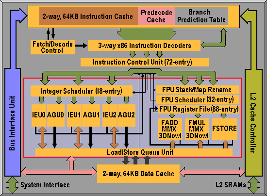
- Superscalar FPU: AMD’s previous CPUs were poor floating-point performers compared with Intel’s. This previous weakness has been more than adequately addressed in the Athlon, which features an advanced three-issue superscalar engine based on three pipelined out-of-order execution units (FMUL, FADD, and FSTORE). The term superscalar refers to a CPU’s ability to execute more than one instruction per clock cycle, and while such processors have existed for some time now, the Athlon represents the first application of the technology to an FPU subsystem. The superscalar performance characteristic of the Athlon’s FPU is partly down to pipelining – the process of pushing data and instructions into a virtual pipe so that the various segments of this pipe can process the operations simultaneously. The bottom line is that the Athlon is capable of delivering as many as four 32-bit, single-precision floating-point results per clock cycle, resulting in a peak performance of 2.4 Gflops at 600MHz.
- Branch Prediction: The AMD Athlon processor offers sophisticated dynamic branch prediction logic to minimise or eliminate the delays due to the branch instructions (jumps, calls, returns) common in x86 software.
- System Bus: The Athlon system bus is the first 200MHz system bus for x86 platforms. Based on the Digital’s Alpha EV6 bus protocol, the frontside bus (FSB) is potentially scaleable to 400MHz and beyond and, unlike the shared bus SMP (Symmetric Multi-Processing) design of the Pentium III, uses a point-to-point architecture to deliver superior bandwidth for uniprocessor and multiprocessor x86 platforms.
- Cache Architecture: Athlon’s cache architecture is a significant leap forward from that of conventional sixth-generation CPUs. The total Level 1 cache is 128KB – four times that of the Pentium III – and the high-speed 64-bit backside Level 2 cache controller supports between 512KB and a massive 8MB.
- Enhanced 3DNow!: In response to Intel’s Pentium III Streaming SIMD Extensions, the 3DNow! implementation in the Athlon has been upgraded, adding 24 new instructions to the original 21 3DNow! instructions – 19 to improve MMX integer math calculations and enhance data movement for Internet streaming applications and 5 DSP extensions for soft modem, soft ADSL, Dolby Digital, and MP3 applications.
The Athlon uses AMD’s Slot A module design, which is mechanically compatible with Slot 1 motherboards but uses a different electrical interface – meaning that Athlon CPUs will not work with Slot 1 motherboards. Slot A is designed to connect electrically to a 200MHz system bus based on the Alpha EV6 bus protocol, thus delivering a significant performance advantage over the Slot 1 infrastructure. As well as providing its own optimised chipset solution – the AMD-750 chipset – the company is working with leading third-party chipset suppliers to assist them in delivering their own Athlon-optimised solutions.
The Athlon was initially available in speed grades of 500, 550 and 600MHz with a 650MHz following a little later, all fabricated using AMD’s 0.25-micron process technology. By the end of 1999 AMD had increased speeds further, its new 750MHz K75 core being the first processor built using the company’s aluminium 0.18-micron, six-layer metal, manufacturing process technology. Whether this can claim to have been the fastest x86 CPU of the millennium is debatable, as Intel was quick to respond with the announcement of an 800MHz Pentium III. However, AMD re-took the lead in the speed stakes early in 2000 with the announcement of 800MHz and 850MHz versions and succeeded in beating Intel to the coveted 1GHz barrier by a matter of days some weeks later.
In fact, the last few processor releases based on the K75 core were a little disappointing in that each increase in clock speed was accompanied by a drop in the L2 cache frequency of the processor, which never peaked above 350MHz. This architectural limitation was soon to be addressed however, with the release of the next iteration in the Athlon line, the Thunderbird, along with its full speed on-die L2 cache.